Stop Guessing Your Wafer Temps
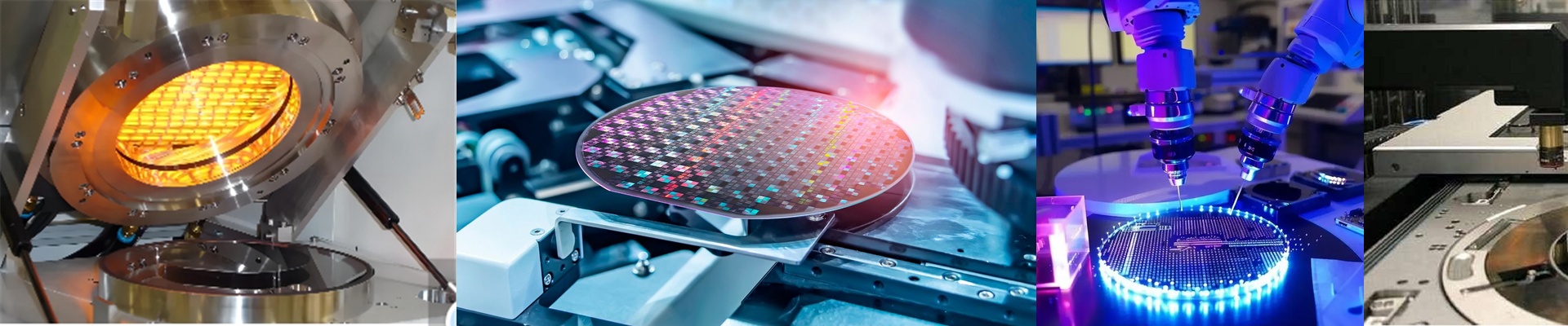
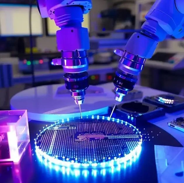
If you’re building a smart fab, you’ve got to ditch the old contact thermocouples. They just don’t cut it anymore. For wafer tools, we’ve moved to high-speed infrared (IR) sensing. It lets us grab real-time thermal maps without ever touching the substrate. If you want your digital twin to actually match what’s happening in the real world, you need a constant stream of high-frequency data. Non-contact sensing is the only way to get it.
The nitty-gritty of IR
It all comes down to Planck’s Law—basically turning infrared radiation into a temperature reading. But here’s the catch: you have to get your emissivity settings right for silicon or GaAs. If those are off, your data is basically garbage. To keep things clean, we use narrow-band pyrometry. It filters out the noise from the heating elements so the sensor focuses on the wafer, not the furnace wall.
Making the data actually useful
These aren’t just fancy gauges sitting on a shelf. We design these sensors to feed raw digital signals straight into your PLC or SCADA system. This is where it gets cool. You get closed-loop PID control. If a hot spot starts to form, you can tweak the power in milliseconds. It’s fast. Really fast. Just a heads-up: this much data can choke a weak network. Make sure you’ve got a high-bandwidth fieldbus, or you’ll be dealing with lag.
The trade-offs (because nothing is perfect)
The upside is huge. No more probe contamination. No more accidental wafer breakage. Your yield will thank you. But there are a few things to watch out for. IR needs a clear line of sight. If your tool has a weird shape or internal shielding, you’re going to have blind spots. You’ve got to be smart about where you place the sensors during the design phase. And then there’s the glass. If your viewport gets cloudy from process byproduct, your readings will start to drift. You’ll need to build in a cleaning cycle or use a gas purge to keep the optics crystal clear.