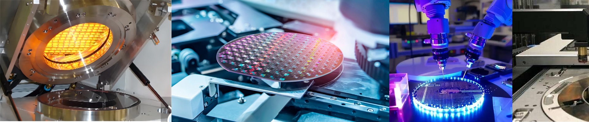
On the fab floor, the photoresist bake isn’t a “warm-up.” It’s the hinge—where line-width control, defect density, and yield get decided. A hotspot during soft bake or hard bake can leave a thinning profile that prints into the resist and sticks around. A cold spot can under-cure, and suddenly the film is vulnerable to stripping and micro-scratches. When thermal uniformity drifts, you don’t get one bad wafer as a warning. You get hundreds of marginal devices that fail reliability hours later. Sustainable fab manufacturing isn’t just about energy use. It’s about running every thermal step with enough precision that you don’t have to over-bake, over-clean, or over-scrap just to hit spec. When infrared heating is engineered for sub-millimeter control of the thermal field, that precision becomes repeatable, low-waste operation.
What matters under the hood: IR accuracy and repeatability
Infrared heating in semiconductor work only matters when the heat arrives at the wafer as a stable, uniform flux. The technical heart is two things: wavelength selection and field uniformity. We use short-wave infrared sources with tight spectral control. The point is rapid, direct coupling into the photoresist and substrate—without loading the chamber with extra thermal mass. That gives you a fast ramp with low thermal inertia, which matters because it cuts overshoot and makes temperature control feel like physics, not guesswork. Then comes uniformity. In practice, we target sub-millimeter uniformity across the wafer, and we want wafer-level temperature control that repeats run after run. That isn’t a slogan; it’s a measurable constraint. It means the hot zone is mapped, the lamp array is matched to the map, and the feedback loop holds the bake profile within tight limits across lots. What you can actually measure is process repeatability: the same temperature profile at the same spot on the wafer, day after day, shift after shift. In a lithography bake stack, that repeatability keeps critical dimensions stable and reduces the need to compensate with recipe tweaks. It also protects thermal budget on advanced nodes, where small excursions can shift threshold voltages and leakage.
Where it pays off: lithography, cleaning, and packaging—without chasing variability
Sustainable gains in the fab show up when you remove variability at the source. Infrared heating with sub-millimeter uniformity does that in the places where heat and cleanliness collide.
Lithography bakes: soft bake and hard bake, without playing guessing games
Photoresist processing lives and dies on the soft bake to remove solvent and set the film, and the hard bake to harden the image before etch or implant. If the bake is uneven, the resist flows differently across the wafer, and CD uniformity drifts. Then you’re chasing bias across the field, stretching exposure latitude, and tightening tolerances that shouldn’t need tightening. With controlled infrared heating, the wafer sees a uniform thermal field. Soft bake becomes consistent solvent removal, and hard bake becomes consistent crosslinking. That consistency cuts rework and scrap, and it lets you run the bake at the minimum energy needed to hit resist spec. Lower energy per wafer, fewer failed lots, and a tighter thermal window.
Cleanroom behavior: keep particle generation at zero under Class 1–100 conditions
A heating system that sheds particles defeats the whole point of the bake. In cleanrooms from Class 1 to Class 100, the hardware has to stay out of the particle story. Infrared sources can be configured with low-outgassing materials and cleanable fixtures, and the heating itself is non-contact. No moving hot air means fewer entrained particles and less turbulence around the wafer. That matters because particles during bake can embed into the resist and survive patterning as defects. It also matters after the bake: you’re not fighting contamination created by the tool. Cleaner bakes translate into fewer cleaning steps, less chemical use, and less downtime spent chasing particle excursions.
Uptime you can bank on: stable output without unplanned stops
Fabs run on uptime. An unplanned lamp change or a temperature loop that drifts stops the line. Infrared systems engineered for reliability hold output steady over long duty cycles. We’ve run units for 5,000+ hours with less than 5% output drop, and the control architecture is built to detect and compensate for aging in real time. Stable output means fewer interruptions for recalibration and fewer recipe adjustments to cover drift. It also means predictable energy use. When the tool isn’t chasing temperature, energy per wafer settles into a narrow band—something you can report, plan around, and reduce without sacrificing throughput.
Packaging and drying: thermal control that doesn’t stress the stack
Semiconductor packaging is plenty sensitive thermally. Delamination risk, warpage, and moisture outgassing all hate hot spots and fast, uncontrolled ramps. Infrared heating delivers localized heat with fast response, so the profile follows the process intent instead of being dragged around by the thermal mass of the fixture. In wafer drying and cleaning, the same principle holds. Controlled infrared heating can drive off moisture without thermal shock, and it can do it without blowing particulates across the surface. That reduces re-contamination and keeps the drying step aligned with the cleanroom environment.
The realities: installation, compatibility, and what you need to plan for
Infrared heating is compact and efficient, but it isn’t plug-and-play into every legacy bake chamber without thinking. The hardware has to match the chamber geometry. Lamp arrays, reflectors, and sensors need a clean line of sight to the wafer plane, and the mounting has to preserve the cleanroom envelope. Integration usually means paying attention to mechanical interfaces, thermal isolation, and EMI shielding. Expect a short commissioning window to map the field and lock the profile to your recipe. Compatibility with existing equipment is straightforward in principle—infrared sources can be adapted to standard tool footprints—but it isn’t universal. Give us chamber dimensions, exhaust paths, and control interface details early. We size the lamp array and control loop to the chamber, not the other way around. One practical trade-off is line-of-sight. Infrared heating is most uniform when the wafer sees a consistent flux. Shadowing from fixtures or edge rings can create edge effects. We handle that with edge-compensated lamp maps and controlled view factors, but it does demand attention to mechanical design. Plan fixturing so the wafer sits fully within the designed field. Another constraint is thermal mass. Infrared heating is fast and responsive, which is an advantage, but it also means the control loop has to be tuned to prevent overshoot during ramps. If your process needs very steep ramps, loop tuning becomes part of the qualification. And maintenance is real. Lamps age. Reflectors degrade. Keep a spare kit and a preventive schedule. The system is built to run continuously, but it still needs scheduled care. If you run a fab, you don’t need promises—you need a thermal step that behaves the same way every time, with energy use you can defend and defects you can keep low. Infrared heating, engineered for sub-millimeter uniformity and repeatable control, delivers that predictability. In a fab, predictability is the most sustainable operating mode you can buy.